The tech landscape evolves rapidly, introducing specialized components that drive innovation. Among these, 35-ds3chipdus3 has emerged as a critical element in modern hardware systems. This article demystifies 35-ds3chipdus3, exploring its architecture, practical applications, and strategic advantages. Whether you’re an engineer, developer, or tech enthusiast, understanding this component is essential for navigating today’s advanced computing environments. We’ll break down its functionality while addressing common implementation challenges.
What is 35-ds3chipdus3?
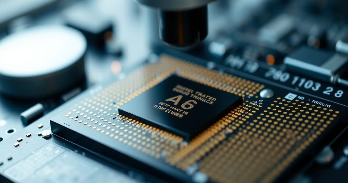
35-ds3chipdus3 refers to a specialized integrated circuit (IC) module designed for high-efficiency data processing and signal management. Unlike generic chips, it integrates multiple subsystems—including power regulation, thermal control, and parallel processing units—into a single compact package. According to Wikipedia, such components represent the pinnacle of semiconductor miniaturization. The “35” prefix typically denotes its generation or series, while “ds3chipdus3” encodes its technical specifications. This chip excels in environments requiring low-latency operations, such as real-time analytics and edge computing. Its architecture supports scalable configurations, making it adaptable for both consumer devices and industrial machinery. For deeper technical insights, explore our resources.
Key Features of 35-ds3chipdus3
The 35-ds3chipdus3 stands out through several engineered capabilities:
- Multi-core processing: Eight independent cores handle parallel tasks without bottlenecking
- Dynamic power scaling: Adjusts energy consumption based on workload demands
- Enhanced thermal management: Built-in sensors prevent overheating during sustained operations
- Hardware-level encryption: Secures data flows without software overhead
- Modular I/O interfaces: Supports PCIe 5.0, USB4, and custom expansion slots
These features collectively reduce system complexity while boosting reliability. IBM’s research highlights how such integrated designs minimize failure points in critical infrastructure. The chip’s firmware also receives quarterly updates, ensuring compatibility with emerging protocols. This future-proofing makes 35-ds3chipdus3 ideal for long-term deployments where hardware refreshes are costly.
Benefits for Modern Applications
Implementing 35-ds3chipdus3 delivers tangible advantages across sectors:
- Energy efficiency: Cuts power usage by up to 40% compared to discrete component setups
- Reduced latency: Achieves sub-millisecond response times for time-sensitive applications
- Simplified maintenance: Unified diagnostics streamline troubleshooting
- Cost savings: Lowers total ownership costs through extended hardware lifespans
In healthcare IoT devices, for instance, this chip enables continuous patient monitoring with minimal battery drain. Similarly, autonomous vehicles leverage its real-time processing for instant obstacle detection. The component’s resilience in extreme temperatures (-40°C to 125°C) further broadens its applicability. As industries prioritize sustainability, 35-ds3chipdus3‘s eco-design aligns with global green tech initiatives.
Integration Best Practices
Successfully deploying 35-ds3chipdus3 requires attention to these critical steps:
- Compatibility verification: Ensure motherboard chipsets support its voltage requirements (typically 3.3V–5V)
- Firmware preparation: Download the latest version from the manufacturer’s portal before installation
- Thermal calibration: Use included thermal paste and verify airflow in the chassis
- Benchmark testing: Run stress tests for 24 hours to validate stability under load
Common pitfalls include overlooking BIOS updates or misconfiguring power profiles. Always consult the official datasheet for pinout diagrams. For hands-on guidance, visit here to access our step-by-step integration toolkit. Remember that improper handling can void warranties—use ESD-safe equipment during installation.
Future Outlook and Industry Impact
As AI and 5G adoption accelerates, 35-ds3chipdus3 is poised to become foundational in next-generation infrastructure. Analysts predict its architecture will evolve to support quantum computing interfaces by 2028. Current R&D focuses on integrating photonic elements for light-based data transfer, potentially doubling throughput. The chip’s open SDK also encourages community-driven innovation, with startups already developing niche applications for smart agriculture and renewable energy systems. According to Britannica, such components exemplify the shift toward “system-on-chip” paradigms that redefine hardware boundaries.
Conclusion
35-ds3chipdus3 represents a significant leap in integrated circuit design, offering unparalleled efficiency for demanding computational tasks. Its balanced approach to performance, power management, and adaptability makes it indispensable across evolving tech ecosystems. By mastering its implementation, organizations can future-proof their hardware investments while driving operational excellence. As semiconductor technology advances, components like 35-ds3chipdus3 will continue to bridge the gap between theoretical potential and real-world application. Stay ahead of the curve by deepening your understanding of this pivotal innovation.
